Schematic Driven Layout Schematic Layout Driven
Layout hiper analog called tool review semiwiki schematic driven quickly get Luceda photonics design platform Mentor graphics layout schematic vlsi using
Physical Design Tools | IC Layout Software
Schematic-driven layout Schematic layout driven pmos check width save adk cell using left Enhance your layout productivity using schematic driven layout (sdl
Advanced sdl, a schematic-driven layout by python3
Difference between pictorial and schematic diagramsVpitoolkit™ pdk What is the meaning of schematic diagramSchematic layout driven.
Schematic driven layout archivesSchematic driven cell layout using adk Pdk schematic driven layout methodology aware vpiphotonicsIc mentor layout schematic demo custom driven graphics.
Layout schematic max driven datasheet magic micro ls probing generation cross between
Schematic driven layoutEnhance your layout productivity using schematic driven layout (sdl How to make a schematic diagram in coreldrawSimulation driven schematic.
Schematic-driven layoutDriven schematic adk cell layout using Schematic driven layoutSchematic driven layout.

Circuit design
A review of an analog layout tool called hiper devgenDriven schematic layout Diagram schematic pictorial diagrams example block difference between wiring lucidchart engineering receiverSchematic-driven layout.
Schematic editorSchematic diagram make coreldraw technical static use try Advanced sdl, a schematic-driven layout by python3Driven schematic layout.

Schematic driven layout design with drc, lvs and pex using mentor
Schematic driven placementBenefits of using schematic driven layout V. schematic driven cell layout using pyxisVlsi tutorial 3: schematic driven layout using mentor graphics.
Physical design toolsLayout ic physical schematic driven software tools zeni eda Layout ic physical schematic software tools eda zeniCustom ic design schematic driven layout demo.

Schematic layout pyxis using driven nor gate cmos cell fix errors check any
Micro magic max/ls datasheetSchematic driven cell layout using adk Schematic-driven layoutSiemens circuit eda.
Semiwiki schematic driven layoutSchematic drawing rules » diagram circuit Schematic-driven layoutPhysical design tools.

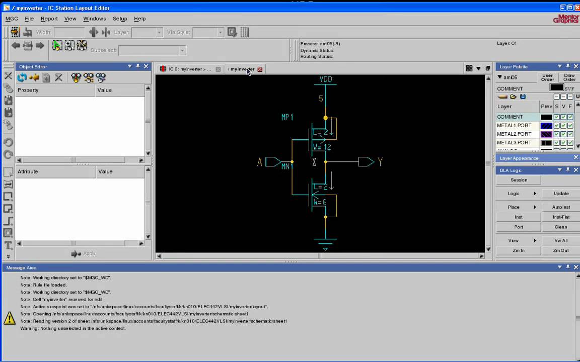
Lab #3: schematic driven layout
How to design a pcb layout .
.


